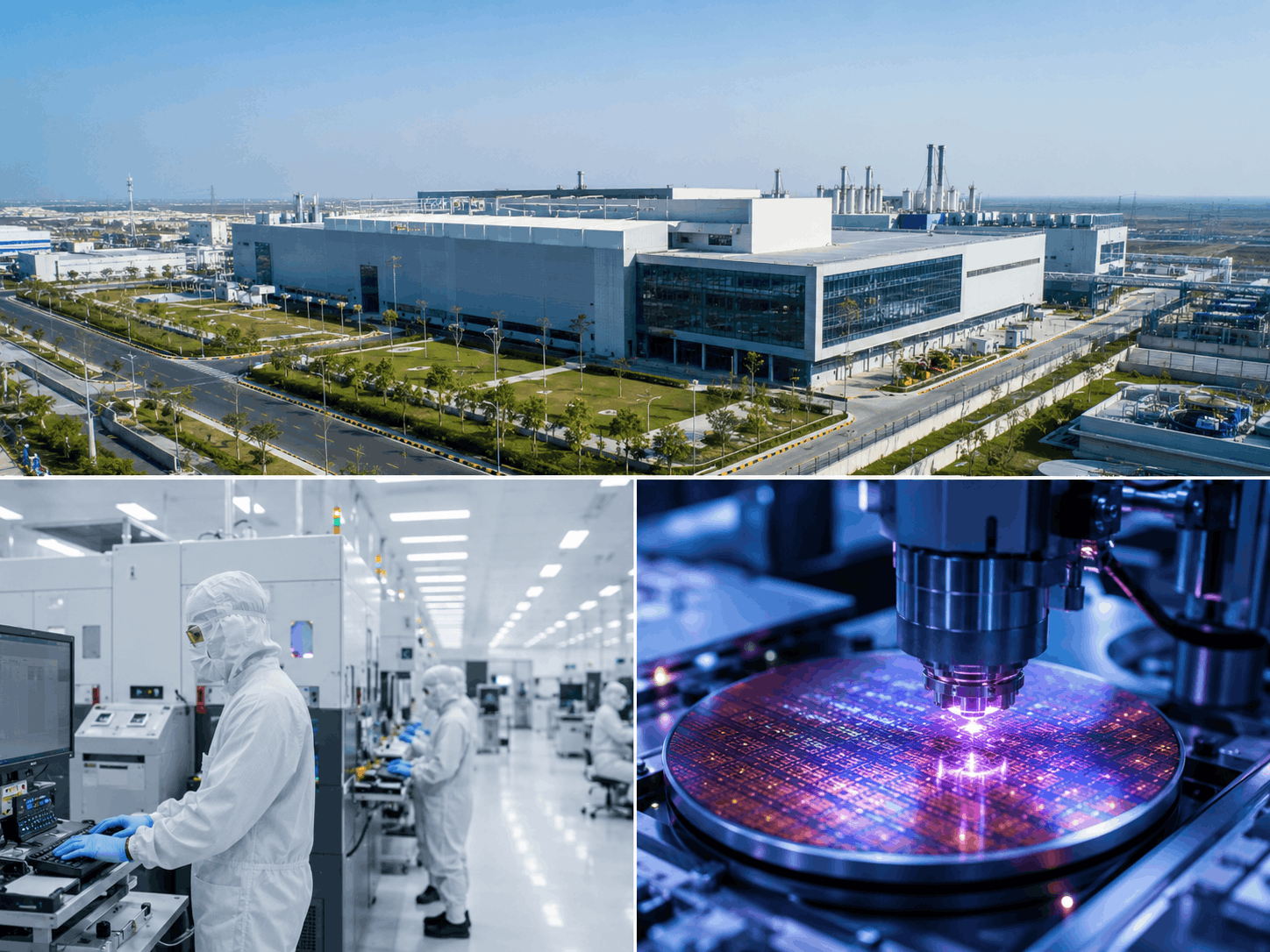
The Tata-ASML Dholera project is a planned $11 billion semiconductor manufacturing facility in Gujarat that aims to strengthen India's domestic chip production and support the country's growing electronics industry.
But what exactly is ASML, and why is its technology considered critical for semiconductor manufacturing worldwide? As Tata Electronics advances its semiconductor facility in Dholera, understanding the role of lithography systems, chip fabrication, and advanced manufacturing technology has become increasingly important.
This article explains the technology behind the project and why it matters for India's semiconductor ambitions.
What Is ASML and Why Is It Important?
ASML is a Netherlands-based technology company that develops advanced lithography systems used by semiconductor manufacturers worldwide.
Its machines function like extremely precise nanoscale printers. These systems transfer circuit patterns onto silicon wafers, allowing billions of microscopic transistors to be created on a single chip.
Without lithography technology, modern semiconductor manufacturing would not be possible.
Today, ASML equipment is used across the global semiconductor industry to produce chips used in:
-
Smartphones
-
Computers
-
Automotive electronics
-
Telecommunications equipment
-
Artificial intelligence systems
-
Industrial automation devices
-
Consumer electronics
How Photolithography Works
Photolithography is one of the most important stages of semiconductor manufacturing. The process involves transferring circuit designs onto silicon wafers layer by layer.
Step 1: Wafer Preparation and Photoresist Coating
The process begins with a polished silicon wafer.
Manufacturers deposit thin layers of materials such as conductors, insulators, or semiconductors onto the wafer depending on the manufacturing stage.
The wafer is then coated with a light-sensitive material called photoresist, which allows circuit patterns to be recorded during exposure.
Step 2: Computational Lithography and Pattern Optimization
Before exposure begins, sophisticated software analyzes and optimizes the circuit design.
Advanced algorithms intentionally modify mask patterns to compensate for optical distortions and manufacturing challenges that occur at nanometer-scale dimensions.
This helps improve pattern accuracy and manufacturing yields.
Step 3: Exposure and Pattern Transfer
A photomask (also called a reticle) containing the circuit blueprint is loaded into the lithography system.
The machine generates high-energy light and projects the circuit pattern onto the wafer.
For advanced chip manufacturing, Extreme Ultraviolet (EUV) systems create light using powerful lasers that strike microscopic droplets of molten tin thousands of times every second.
Ultra-precise mirrors then shrink and focus the pattern before transferring it onto the photoresist-coated wafer.
Throughout the process, the machine continuously aligns the wafer and mask with extraordinary precision to ensure accurate layer placement.
Step 4: Development and Etching
After exposure, the wafer undergoes chemical development.
The exposed portions of the photoresist are removed, revealing the circuit pattern.
Manufacturers then etch the exposed areas to create microscopic semiconductor structures.
This process is repeated dozens or even hundreds of times until the complete integrated circuit is formed.
Semiconductor Manufacturing Process Overview
Tata Electronics and the Dholera Semiconductor Facility
According to publicly reported information, Tata Electronics is developing a semiconductor fabrication facility in Dholera, Gujarat.
The project is valued at approximately $11 billion and is planned as a 300mm wafer fabrication facility, making it one of India's largest semiconductor manufacturing investments.
Industry reports indicate that the facility may target production capacity of approximately 50,000 wafers per month.
The facility is expected to manufacture semiconductor chips for a wide range of industries, including:
-
Artificial intelligence
-
Automotive electronics
-
Consumer devices
-
Telecommunications
-
Industrial automation
-
Power management systems
The project forms part of India's broader effort to strengthen domestic semiconductor manufacturing capabilities and reduce dependence on imported chips.
Key Reported Details of the Project
The facility is expected to focus primarily on mature semiconductor technologies ranging from approximately 28nm to 110nm, which remain widely used across numerous industries.
DUV vs EUV Lithography
ASML manufactures multiple categories of lithography systems.
DUV systems are commonly used for large-scale commercial manufacturing and are expected to play an important role in mature-node semiconductor production.
EUV systems are among the most advanced manufacturing machines in existence and are used to produce cutting-edge chips containing billions of transistors.
Industry estimates suggest that advanced EUV systems can cost hundreds of millions of dollars per machine due to their engineering complexity.
Workforce and Employment Impact
Semiconductor manufacturing facilities require highly skilled teams working continuously to support production operations.
Industry reports suggest that advanced lithography systems may require support from multiple specialists including engineers, operators, and maintenance teams.
Key Roles in Semiconductor Manufacturing
Because semiconductor fabrication plants operate 24 hours a day, staffing is typically organized across multiple rotating shifts.
Large semiconductor projects also create employment opportunities across engineering, construction, logistics, utilities, technical services, and support industries.
Publicly reported estimates suggest that the broader ecosystem associated with the Dholera semiconductor project could support thousands of direct and indirect jobs over time.
Why Dholera Was Chosen
Semiconductor manufacturing requires extensive infrastructure support.
Key requirements include:
-
Reliable electricity supply
-
Water infrastructure
-
Transportation connectivity
-
Industrial land availability
-
Logistics networks
-
Digital infrastructure
Dholera's planned industrial ecosystem, transportation projects, and integrated utility infrastructure have made it one of the locations frequently discussed in relation to semiconductor manufacturing development in India. These advantages are part of the broader vision behind Dholera Smart City, which has been planned as a major industrial and infrastructure hub in Gujarat.
Frequently Asked Questions (FAQs)
What is ASML?
ASML is a technology company that develops lithography systems used in semiconductor chip manufacturing.
What is photolithography?
Photolithography is a manufacturing process that transfers circuit patterns onto silicon wafers to create semiconductor chips.
What is the Tata Electronics semiconductor project in Dholera?
It is a planned semiconductor fabrication facility in Dholera, Gujarat, designed to support domestic chip manufacturing.
What production capacity is planned for the Dholera facility?
Industry reports indicate a target capacity of approximately 50,000 wafers per month.
What is the difference between DUV and EUV lithography?
DUV is commonly used for mature semiconductor manufacturing, while EUV is used for more advanced semiconductor nodes.
Why was Dholera selected for semiconductor manufacturing?
Dholera offers planned industrial infrastructure, transportation connectivity, utility systems, and land availability required for large-scale manufacturing facilities.
Conclusion
The Dholera semiconductor project represents an important development in India's efforts to build a stronger domestic semiconductor ecosystem. Supported by advanced manufacturing technologies and infrastructure planning, the facility is expected to contribute to semiconductor production, workforce development, and industrial growth.
As discussions around semiconductor manufacturing continue to evolve, understanding technologies such as ASML lithography and the requirements of modern chip fabrication provides valuable insight into how advanced electronics are produced and why projects like Dholera are attracting national attention.